












![[FA] SIT One SITizen Alumni Initiative_Web banner_1244px x 688px.jpg](/sites/default/files/2024-12/%5BFA%5D%20%20SIT%20One%20SITizen%20Alumni%20Initiative_Web%20banner_1244px%20x%20688px.jpg)
Electronics and Data Engineering graduate Charlotte Wong shares how her Integrated Work Study Programme at global MNC AMD helped her discover a passion for chip layout design, setting her up for a thriving career in the sector.

Charlotte Wong (third from the left) with the AMD Singapore office team she worked with during her IWSP. (Photo: Charlotte Wong)
Imagine spending hours painstakingly tinkering with the design of microchips to ensure they are production-ready, only for them to fail during testing.
Microchips, which pack billions of microscopic transistors into a tiny piece of silicon, are the foundation of the digital world. They power everything from smartphones and game consoles to cars and medical equipment.
For Charlotte Wong, this was not a hypothetical. During her eight-month Integrated Work Study Programme (IWSP) with global semiconductor company Advanced Micro Devices (AMD) in 2024, designing them took a lot of trial and error. Through SIT's IWSP, students spend extended periods embedded in industry, working on real projects while earning academic credit. The experience would not only sharpen her technical skills but also give her clarity on the direction of her career.
Microchip layout design, she soon realised, was an exercise in patience.
“At first, I thought that once the circuit design was ready, the layout would fall into place,” said Charlotte, who was then pursuing a Bachelor of Engineering with Honours in Electronics and Data Engineering (EDE) at SIT. “But in reality, the first version often did not meet the performance target.”
Sparking a Passion
That frustration turned into fascination, but it didn’t happen overnight. As an integration layout engineer at AMD, Charlotte used computer software to lay out the intricate circuits of semiconductor chips according to a blueprint. She would then subject the chips to rigorous checks to ensure they met performance and manufacturing requirements.
The learning curve was steep, as it was her first time working on microchip layouts in a real-world setting. To complicate matters, the chips contained different materials, from polysilicon to metals.
“At first, I didn’t understand how each layer of the chip worked, and how to route the signals,” she said. But she eventually figured it out by observing her colleagues and practising on the job.
Technical challenges aside, Charlotte also had to overcome her shy nature. And her growth in both her technical capabilities and professional maturity did not go unnoticed by her supervisors.
"Over the course of Charlotte's eight-month internship, Charlotte became more confident in her abilities, adapted well to new challenges, and consistently demonstrated her willingness to learn. It was rewarding to see her develop into a capable member of our team,” said Jesca Benitez, Charlotte's IWSP Supervisor at AMD.
Charlotte also credits the engineering fundamentals she built through her EDE programme, including Semiconductor Physics, Semiconductor Devices and Reliability and Semiconductor Fabrication, which proved invaluable in the workplace. So did the laboratory sessions, group projects and industry-focused assignments she did at SIT, which helped her develop a systematic approach to problem-solving, while honing her communication and time management skills.
“There were also industry visits to leading semiconductor companies in Singapore, which gave me a clearer picture of how the local ecosystem functioned at scale," said Charlotte.
Still, nothing beats the pressure of real-world experience.
“Being at AMD taught me to pay close attention to detail,” she said. “For example, I might just be working on a chip’s transistor. But if that small component does not function correctly, the entire chip fails, and it could end up in products worldwide. That showed me how small details mattered a lot.”
More importantly, the experience gave Charlotte clarity about the kind of engineer she could become.
“Initially I was more interested in machine learning and data-related roles, but AMD made me realise how much I really enjoyed layout design. No day is boring, because there is a lot of problem-solving involved,” said Charlotte, who also bonded with co-workers over their shared interests such as anime and video games.
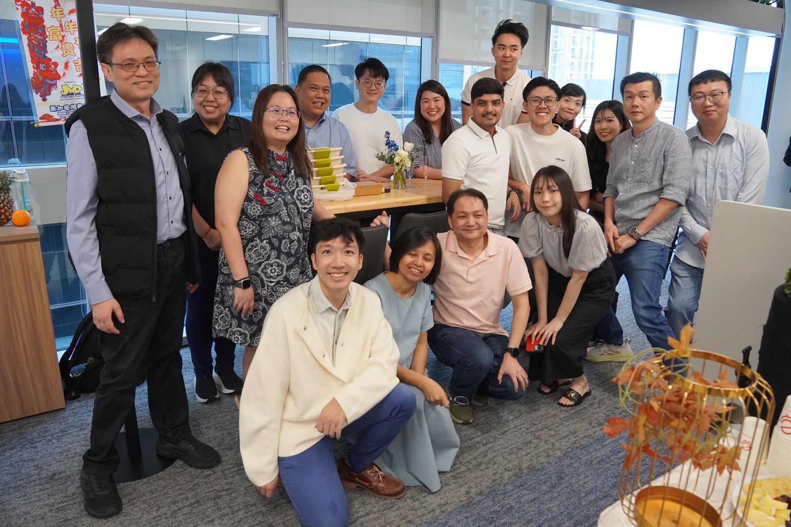
Charlotte (front row, extreme right, semi-squatting) at the Astera Labs Singapore office with her colleagues. (Photo: Charlotte Wong)
From Intern to Engineer
Her IWSP at AMD provided a solid foundation in chip layout design, giving her an edge in her next role.
Shortly after graduating in 2025, she took up a full-time job as an analog layout engineer at Astera Labs, an American semiconductor manufacturer and artificial intelligence company.
“I felt much more confident entering my first full-time role because I'd already experienced what it was like to work in a global engineering team,” she noted.
Now Charlotte is paying it forward. After taking a year off during university to recharge, she returned with a clearer sense of purpose, and today is an alumni mentor to her juniors at SIT.
“I understand how tough it feels when school doesn’t go according to plan,” Charlotte said. “I hope to encourage my mentees to keep going even when things are uncertain and show them that resilience and effort matter more than being perfect.”
So what does an analog layout engineer actually do? Charlotte shares more about her work at Astera Labs here.